Start with informal specification of desired system
Notes are for post midterm material.
A circuit whose outputs are Boolean functions of its inputs is a combinational circuit.
For speed, use 2-level implementations, for minimization, use simplified expressions.
Half Adders sum two inputs and has two outputs, S (sum, with XOR gate) and C (carry, with AND gate).
Full Adder sums three inputs. Implemented with two half adders and an AND gate.
Decoders can, for example, take 3 inputs to 8 outputs, with 8 AND gates.
Encoders take 8 inputs and binary representation of the selected input in terms of three outputs (z = d1 + d3 + d5 + d7, y = d2 + d3 + d5 + d7, x = d4 + d5 + d6 + d7).
Multiplexers are switches that connect selected inputs to their outputs. Can be used to implement any function of n variables with a 2^(n-1)-to-one-line multiplexer.
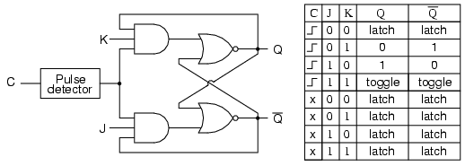
Sequential Circuits contain memory elements. Mealy machine output depends on inputs AND the state of memory elements. Moore machines' outputs depend only on the current state. Uses circuit feedback. A circuit that is a loop with two NOT gates (using feedback) holds two steady states Q and Q'.
Flip-Flops use "edge-triggered" enabler inputs to allow time for the combinational logic outputs to reach their correct values, simultaneously. These are sequential using the clock signal.
Positive edge triggering enables when the signal goes from 0 to 1. Negative edge triggering enables when the signal goes from 1 to 0.
A(t+1) = J•A'(t) + K'•A(t). Sets for J, resets for K.Characteristic tables are truth tables where outputs can be written as state prior to triggering as Q(t) and after triggering as Q(t+1). Same with characteristic equations.
Flip flops having timings:
Clock driven circuits with memory elements.
One design procedure, given state diagram or state specifications:
If given circuit:
State Assignment is identifying each state as a binary string. These binary strings represent each flip flop that stores a bit:
| State | Binary | Gray Code | One-Hot |
|---|---|---|---|
| a | 000 | 000 | 00001 |
| b | 001 | 001 | 00010 |
| c | 010 | 011 | 00100 |
| d | 011 | 010 | 01000 |
| e | 100 | 110 | 10000 |
Excitation Tables are convinient for JK and T flip-flops. They show how to drive desired state transitions. For JK flip-flops:
| Q(t) | Q(t+1) | J | K |
|---|---|---|---|
| 0 | 0 | 0 | X |
| 0 | 1 | 1 | X |
| 1 | 0 | X | 1 |
| 1 | 1 | X | 0 |
JK flip-flop implementation:
Excitation Tables are very important for circuit analysis. They are the core tool for reasoning out a circuit's state diagram. In more complex excitation tables, header might look like:
| Present State, Inputs | Next state, Flip flop inputs |
|---|
Or inputs can be moved into the header to make the table shorter:
| Present state | Next State | based on X | Output Z | based on X |
|---|---|---|---|---|
| X=0 | X=1 | X=0 | X=1 |
States can be reduced by merging states with the same outputs (based on input) or if they are equivalent by the property of state equivalence:
Registers are a collection of flip-flops that store a collection of bits.
Counters a class of registers that cycle through predetermined state sequences.
Parallel Loading allows a circuit to load all information simultaneously (and synchronously using a clock) into the register. n-bit register with parallel load can be implemented with n 2-to-one multiplexers, that choose between read/write (load), and n D flip-flops which store the n bits.
Shift Registers shift information to neighbouring cells. With two (first takes input from itself, second also takes input from first), serial transfer can be done to copy information from one register to another.
Universal Shift Register can shift both ways, implemented using 4 4x1 MUX for state selection and a 4 bit register. (states 3: parallel inputs, 2: shift left, 1: shift right, 0: read/hold)
Ripple Counters use negative edge triggered T flip-flops whose outputs feed into the next flip-flop's clock input. All T inputs are set by input LOGIC. They are non synchronous and use the clock input to ripple instead.
Synchronous Counters use T flip flops, clock driven. A given flip flop will toggle if all previous values are 1. Counter can also be implemented with parallel load, allowing counter to be set to a value.
Bi-directional counters use T flip-flops. Flip flop will toggle if all previous flip flops are 1 and going up, or if all previous flip flops are 0 and going down.
Counters with parallel load can be implemented with JK flip flops.
Memory decoding is converting address lines to appropriate select inputs for an array of binary cells. For a binary cell, SR latch with input, select, read/write mode and output. For a selected cell:
Error detection and correction is used to increase reliability of memory.
Hamming Code defines parity conditions. When checking parity, set an associated "check bit" to 0 if parity is correct, 1 otherwise.
ROM element has k inputs (address) for 2^k • n bits of ROM and n outputs.
AND arrays and OR arrays operate on rows of inputs depending on the address line. An array is programmed by blowing all fuses in the array except for those crossed out with X's, denoting an intact fuse. Programmable Logic Device (PLD) have 3 types:
For a PLA, each input goes through a buffer-inverter gate (triange with two outputs one is inverted, output synchronously), the AND array has 2n columns for n inputs, and k rows (the AND gates) for k product terms. The intersections marked with X's are used for a product term. Each OR gate going vertically in the second array sums the product terms marked with X's to define a function.
PLA Programming table, for F1 = AB + AC and F2 = AC + A'B'C':
| Product term | Inputs | Output Functions |
|---|
| term | A | B | C | F1 | F2 |
|---|---|---|---|---|---|
| AB | 1 | 1 | - | 1 | - |
| AC | 1 | - | 1 | 1 | 1 |
| A'B'C' | 0 | 0 | 0 | - | 1 |